Full-Time


Seiji Samukawa (Fellow, IEEE) received the B.S. degree in instrumentation engineering from Keio University, Tokyo, Japan, and the Ph.D. degree in instrumentation engineering from Keio University in 1992. After the B.S. degree, he joined NEC in 1981. He worked on the research and development of ultra-precise plasma etching processes for ULSI devices and was later promoted to Principal Researcher with Microelectronics Laboratory, R&D Group NEC Corporation. In July 2000, he was a Full Professor with Tohoku University, Sendai, Japan, where he worked with the Innovative Energy Research Center, Institute of Fluid Science. He was also a Principal Investigator with the Advanced Institute of Materials Research (AIMR), Tohoku University, and was a Foreign Chair Professor with Taiwan National Yang Ming Chiao Tung University, Taiwan. Since August 2022, he has been a Chair Professor with Taiwan National Yang Ming Chiao Tung University, where he is currently with the SiC Research and development Center/Neutral Beam Process Research Center. His significant scientific achievements have earned him an Ichimura Award in 2008 in the New Technology Development Foundation, Prizes for Science and Technology, a Commendation for Science and Technology by the Minister of Education, Culture, Sports, Science and Technology in 2009, a Plasma Prize from the American Vacuum Society in 2010, and designation as an IEEE NTC Distinguished Lecturer in 2019. Additionally, he has been elected as a Distinguished Professor of Tohoku University, a Fellow of the Japan Society of Applied Physics since 2008, Fellow of the American Vacuum Society since 2009, and Fellow of the Institute of Electrical and Electronics Engineers since 2018.
Personal Information:
B.S. in Instrumentation Engineering, Keio University (Yokohama, Japan), 1981.
Ph.D. in Instrumentation Engineering, Keio University (Yokohama, Japan) 1992.
Title of a thesis for a doctorate:
“Sub μm Etching of Semiconductors by using Electron Cyclotron Resonance Plasma”.
Prof. Seiji Samukawa is the director of a group working on the fundamental research of plasma etching, plasma CVD and beam technologies for ULSI and the other devices. To realize charge-free and radiation damage-free processes, a new neutral beam generation system has been developed. He found that the neutral beams were efficiently generated by accelerating negative ions in the pulsed plasma. Using the neutral beam processing, he successfully demonstrated sub-50nm damage-free gate electrode etching, damage-free Si channel etching for 45 nm fin-FETs (2005), ultra-thin gate dielectric film formation for 32 nm fin-FETs (2009), damage-free low dielectric film deposition for 22 nm FETs (2009), damage-free Ge etching and oxidation for diamond-shaped Ge nanowire FET (2015) and for sub-7 nm Ge fin-FETs (2016), low temperature damage-free oxidation for high-performance IGZO TFT (2016), damage-free AlGaN etching for high speed AlGaN/GaN HEMTs (2016), and low-damage surface modification of carbon materials (including nanotubes, graphenes and organic moleculers) (2010) for future nanodevices. Additionally, the pulse-time-modulated plasma is also investigating for precise etching and deposition in high sensitive CCD (2003) and MRAM (2007) in production lines. On-wafer monitoring and sensing systems are also developed for precise control of plasma, beam and atom manipulation processes on surfaces. Additionally, plasma vacuum ultra-violet irradiation impinging on the wafer surface is characterized both qualitatively and quantitatively during etching and deposition processes. More recently he has investigated processing technologies based on the combination of biotechnology with neutral-beam-based nano-processes, i.e., bio-nano processes, for future nanoelectronics devices and successfully achieved the fabrication of sub-10-nm-diameter and high density nanodisk (Si, Ge, GaAs, InGaN, Graphene) array structures (2014). The quantum effects of these nano-scaled structures were shown to manifest themselves at room temperature due to the damage-free etched surfaces made possible by the neutral beam etching processes.
Now, by using these nanodisk structures, he is actively developing “Novel Quantum Effect Devices”, such as high energy conversion efficiency Si quantum dot solar cells, high efficiency thermo-electric conversion device and high efficiency all wavelength quantum dot LEDs. Now, he is director of Innovative Energy Research Center of Institute of Fluid Science, Tohoku University since 2013. He is also principal investigator (PI) in The World Premier International Research Center Initiative (WPI), Advanced Institute for Materials Research (AIMR) of Tohoku University since 2012, deputy director of Material Solutions Center (MaSC) Tohoku university since 2013, director of Core Technology Consortium for Advanced Energy devices of Tohoku university since 2013, Joint appointment Fellow of National instituite of advanced industrial science and technology (AIST) since 2015, Chair Professor of National Chiao Tung University (Taiwan) since 2014 and also Renowned Overseas Professor of Shanghai University of Engineering Science since 2018.
In recognition of his excellent achievements outlined above, he has been elected as a “Distinguished Professor” (2% in full professors) of Tohoku University, “Fellow” of the Japan Society of Applied Physics (JSAP), American Vacuum Society (AVS) and also The Institute of Electrical and Electronics Engineers (IEEE) since 2008, 2009 and 2018, respectively.
July 1994 to June 2000. LSI Basic Research Laboratory, Silicon Systems Research Laboratories, Principal Researcher of a group working on the fundamental research of advanced plasma etching processes for sub 0.1 μm technology, built on the damage-free high-performance etching technique. Responsible also for the development of plasma diagnostics to be used on. For large scaled substrate of more than 12 inches, a new ultra-high frequency (UHF, 500MHz) plasma source with a spokewise antenna has been developed. Passing from sub-micron dimension device technologies to sub-100nm in the early mid-1990s coupled with thinning gate dimensions brought device damage considerations to the fore. His major contribution addressed the requirement for ultralow plasma potentials and electron temperatures along with superior species flux uniformity to reduce damage. This contribution, the 500 MHz (UHF) spoke antenna inductively coupled plasma source achieved these goals and foretold the emergence of what is today’s ultrahigh frequency plasma sources, capacitively coupled VHF and microwave-based that are critical for damage-free plasma processing. High-performance gate electrode and Al electrode patterning of sub-0.1μm could be satisfied with the UHF plasma. Additionally, to simultaneously realize damage-free and microloading-free high aspect contact hole patterning, the novel gas chemistry (alternative gas chemistries to PFC) has been developed in the UHF plasma.
July1992 to June 1994. LSI Basic Research Laboratory, Silicon Systems Research Laboratories, Assistant Manager responsible for developing charge-build-up-damage-free etching processes for the next generation to be used with 0.1μm and 0.25 μm ULSI technologies. The pulse-time-modulated plasma (at the pulse timing of μsec) has been innovated in 1992 and the method was investigated in many plasma etching systems. The most important problems with the low-pressure, high-density plasma etching method that was the mainstream etching technology used in manufacturing MOS LSI devices in around 1990 included breakdown of the MOS gate insulation layer by the electrical charge (positive ions) from the plasma that accumulates on the substrate surface and severe degradation of the interface (interface defects and channel mobility, etc.). To address those problems, Dr. Seiji Samukawa performed a detailed analysis of the internal state of the plasma and the mechanism for MOS device degradation and applied the results to invent a pulse time modulated plasma etching technique that uses a pulse period of several tens of microseconds. The technique was subsequently implemented in a mass production system that was developed in collaboration with an equipment manufacturer and tested for practicality in production by LSI manufacturers in Japan and abroad. Its use as a mass production etching process has since spread worldwide. Currently, etching systems that apply this technique are being marketed by three equipment manufacturers and an international market share on the 50% level has been achieved.
July 1989 to June 1992. ULSI Device Development Research Laboratories, Assistant Manager responsible for developing advanced ECR plasma source for the next generation to be used with 0.5μm and 0.35μm ULSI technology. Low energy, high-density, excellent uniform and collimated ions could be generated by optimizing the magnetic field profiles and microwave penetrations in his developed Electron Cyclotron Resonance (ECR) plasma source in collaboration with ANELVA corporation. High-performance gate electrode and interlayer dielectric film (for example, polyimide film) patterning could be accomplished by using the etching system. The system has been introduced in NEC production lines (Yamagata, Sagamihara). Based on these achievements, he received a Ph.D. in Instrumentation Engineering from Keio University in 1992. The title of a thesis for a doctorate was “Sub μm etching of semiconductors by using ECR plasma”.
April 1981 to June 1989. 2nd LSI Division, Process Engineer responsible for developing plasma etching processes for the consumer LSI devices. He started up three advanced semiconductor production factories in NEC Yamagata.
April 2008 to 2013, Principal Researcher for Bio Electoromechanical Autonomous Nano Systems Laboratory (BEANS) (Akihabara, Tokyo, Japan).
June 1998, Visiting Scientist, Bell Laboratories, Lucent Technologies (Murray Hill, NJ, USA).
April 1997 to June 2000, Chief Researcher for Plasma Technology Laboratory in Association of Super-Advanced Electronics Technologies (ASET) (Yokohama, Kanagawa, Japan).
AWARDs
1). Outstanding Paper Award in International Conference on Micro and Nano-Technology (1997), “Effects of discharge frequency on ion current density and etching characteristics in high density plasma.”.
2). Ishiguro Award (for meritorious deed) in R&D Group of NEC Corporation (1998), “for development of damage-free and precise pulse plasma processing techniques.”.
3). Best Review Paper Award in Japan Society of Applied Physics (2001), “Effects of Discharge Frequency in Plasma Etching and Ultrahigh-Frequency Plasma Source for High-Performance Etching for Ultra-large-Scale Integrated Circuits.”.
4). JJAP Editorial Contribution Award in Japan Society of Applied Physics (2003).
5). Plasma Electronics Award in Japan Society of Applied Physics (2004), “for development of damage-free pulse plasma processing techniques.”.
6). Distinguished Graduate Award in Keio University (2005) “for development of ultra-precise plasma etching technologies for advanced semiconductor devices.”.
7). Ichimura Award in the New Technology Development Foundation (2007), “for development of damage-free and precise plasma pulse plasma processing techniques.”.
8). Distinguished Professor in Tohoku University (2008-2011)
9). Fellow Award of Japan Society of Applied Physics (2008), “for development of damage-free and precise plasma processing techniques.”
10). JJAP Best Paper Award in Japan Society of Applied Physics (2008), “Surface Reaction Enhancement by UV irradiation during Si Etching Process with Chlorine Atom Beam.”
11). Prizes for Science and Technology, The Commendation for Science and Technology by the Minister of Education, Culture, Sports, Science and Technology (2009), “for development of ultra-precise plasma etching technologies for eliminating degradation of devices performance.”.
12). Fellow Award of American Vacuum Society (2009) “for development of innovative plasma sources and damage-free pulse plasma processing techniques.”.
13). Plasma Electronics Award in Japan Society of Applied Physics (2010), “for development of on-wafer monitoring and sensing systems for precise control of plasma processes on surfaces.”
14). JJAP Best Paper Award in Japan Society of Applied Physics (2010), “Two-Dimensional Si-Nanodisk Array Fabricated Using Bio-Nano-Process and Neutral Beam Etching for Realistic Quantum Effect Devices.”.
15). STARC Joint Research Award in Semiconductor Technology Academic Research Center (2010), “for development of Super-low-k value SiOCH interlayer dielectric film formation”.
16). Plasma Prize in Plasma Science and Technology Division of American Vacuum Society (2010), “for ground-breaking contributions to the innovative plasma sources that have advanced the discipline of plasma materials processing.”
17). Distinguished Professor in Tohoku University (2011-2014).
18). Principal Investigator (Distinguished Professor) of Advanced Institute for Materials Research (AIMR) in Tohoku University (2012-present).
19). Best Poster Award in IEEE Photovoltaic Specialists Conference, “Effect of Miniband Formation in a Quantum Dot Super Lattice Fabricated by Combination of Bio-Template and Neutral Beam Etching for High Efficiency Quantum Dot Solar Cells”, (The 40th IEEE Photovoltaic Specialists Conference, 2014/06/10) .
20). Best Paper Award in IEEE International Electron Devices and Materials Symposium, Miniband Dependence on the Density of Ge/Si Quantum Dots for Solar Cell Application (IEEE International Electron Devices and Materials Symposium 2015, 2015/11/20)
21). Best Paper Award in IEEE NANO 2016, “Defect-Free Germanium Etching for 3D Fin MOSFET Using Neutral Beam Etching.” IEEE 16th International Conference on Nanotechnology, 2016/08/25)
22) Fellow Award of IEEE (2018), "for contributions to damage-free plasma processing for nano-device manufacturing.”.
23) IEEE Distinguished Lecturers, ” Creating Green Nanostructures and Nanomaterials for Advanced Energy Nanodevices”, (IEEE NTC, 2019)
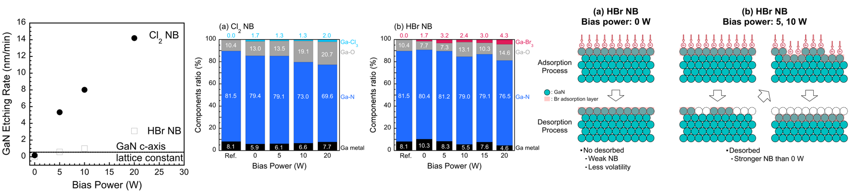
In the gate-recess formation process in AlGaN/GaN HEMTs, normally-off operation is achieved by removing the barrier layer by dry etching to reduce the two-dimensional-electron-gas concentration under the gate electrode. An atomic-layer defect-free etching of GaN is thus indispensable to achieve high-frequency, high-power, and normally-off operation. More-precise atomic-layer defect-free GaN etching was investigated by using an HBr neutral beam. This investigation found that the HBr neutral beam could achieve more-precise atomic-layer etching than the Cl2 neutral beam because the HBr chemistry can control the reactivity of atomic-layer etching by forming a thinner and less-volatile reaction layer.
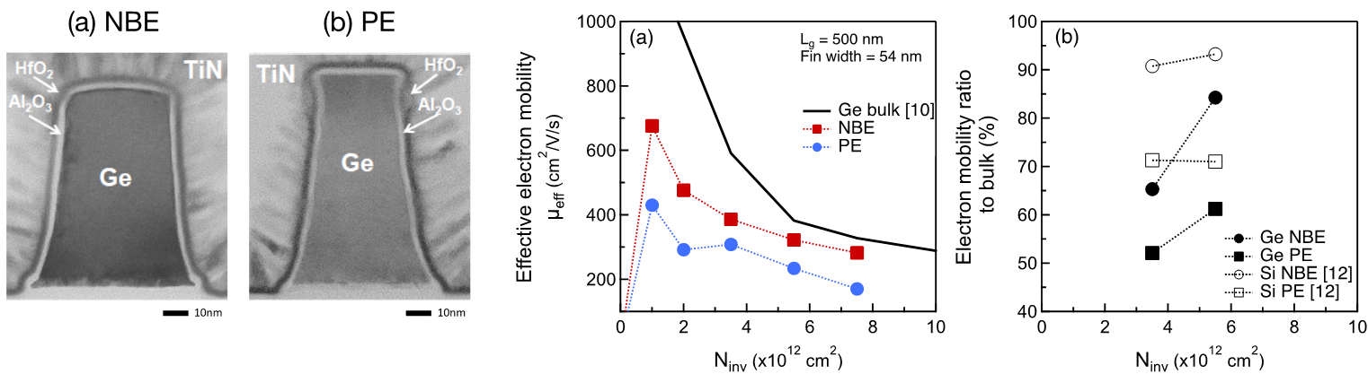
We investigated a high electron mobility Ge FinFET fabricated by defect-free and roughness-free atomic layer neutral beam etching (NBE) compared with one fabricated by conventional plasma etching (PE). The etching interface roughness and defect were estimated by high-resolution transmission electron microscopy (TEM). In the case of using atomic layer defect-free NBE, the root-mean-square roughness of the Ge Fin sidewall surface is 1/3 times smaller than that using PE. Then, the electron mobility of Ge FinFET was improved by 1.65 times compared with that of a PE etched FinFET sample. For the subthreshold swing, the defect density of the interface between the Ge and gate dielectric film was improved by NBE. Ioff average currents of NBE and PE were around 18.1 and 57.6 nA/µm, respectively. As a result, NBE reduces the off-leakage current to 1/3 times less than PE. This corresponded to the differences in surface roughness and defect generation between NBE and PE. Therefore, we found that NBE could achieve a good performance by defect-free and atomically-flat etching the surface.
For the first time, we have demonstrated heterogeneous complementary FETs (hCFETs) with Ge and Si channels fabricated using our neutral beam technologies. The 3D channel stacking integration utilizes two key technologies to bond Ge channels onto Si wafers: 1) atomically defect-free/roughness-free neutral beam thinning processes and 2) a low-temperature (200 °C) hetero-layer bonding technique (LT-HBT) implemented by a surface activating chemical treatment at room temperature. The neutral beam thinning technique we developed was able to obtain the Rtm (mean of maximum peak to valley height) of less than 0.39 nm, the uniformity of Ge thinning depth of less than±0.75 nm, and the thinning rate of 15.3 nm/min. These results demonstrate that our neutral beam technology can obtain atomic-layer-uniform and roughness free Ge etching for the bonding surface. We also implemented a multi-channel structure consisting of two-channel Si and one-channel Ge to obtain a symmetric performance in n/p FETs. Wafer-scale LT-HBT was successfully demonstrated, thus opening the door to new opportunities for ultimate device footprint scaling with heterogeneous integration.
https://scholar.google.com/citations?user=_3GxD78AAAAJ&hl=en
https://scholar.google.com/citations?user=_3GxD78AAAAJ&hl=en
1. S. Samukawa, US Patent-5013401, Microwave Plasma Etching Method and Apparatus
2. S. Samukawa, US Patent-5366586, Plasma Formation using ECR and Method for Processing Substrate by using the Same.
3. S. Samukawa, US Patent-5401351, RF Plasma Etching Apparatus
4. S. Samukawa, US Patent-5468341, Plasma etching method and therfeor
5. S. Samukawa, Kibatsu Shinohara, Hirobumi Matsumoto, Tsutomu Tsukada and Yukito Nakagawa, US Patent-5565738, Plasma Formation using Spokewise Antenna
6. K. Kinoshita and S. Samukawa, US Patent-5744796, Mass spectrometer and radical measuring method
7. K. Kinoshita and S. Samukawa, US Patent-5818040, Neutral particle beam irradiation apparatus
8. S. Samukawa, US Patent-5827435, Plasma processing method and equipment used therefor.
9. S. Samukawa, Tsutomu Tsukada, Yukito Nakagawa, Kibatsu Shinohara, and Hiroyuki Ueyama, US Patent-5900699, Plasma Generator with a Shield Interposing Antenna.
10. S. Samukawa, T. Tsukada, Y. Nakagawa, K. Shinohara, H. Matsumoto, and H. Ueyama, US Patents-5936352 Plasma processing apparatus for producing plasma at low electron temperatures
11. S. Samukawa, Y. Nakagawa, H. Sato, T. Tsukada, K. Shinohara, and Y. Niimura, US Patents-6043608 Plasma processing apparatus
12. H. Ohtake and S. Samukawa, US Patent-6054063 Method for plasma treatment and apparatus for plasma treatment
13. S. Samukawa and K. Tsuda, US Patent-6177147 Process and apparatus for treating a substrate
14. S. Samukawa, US Patent-6348158 Plasma processing with energy supplied
15. K. Ichiki, K. Yamauchi, H. Hiyama, and S. Samukawa, US Patents-6849857 Beam processing apparatus
16. K. Ichiki, K. Yamauchi, H. Hiyama, and S. Samukawa, US Patents-6858838 Neutral particle beam processing apparatus
17. K. Ichiki, K. Yamauchi, H. Hiyama, and S. Samukawa, US Patents-6861642 Neutral particle beam processing apparatus
18. K. Ichiki, K. Yamauchi, H. Hiyama, and S. Samukawa, US Patents-6861643 Neutral particle beam processing apparatus
19. S. Samukawa, K. Ichiki, K. Yamauchi, and H. Hiyama, US Patents- 6909086 Neutral particle beam processing apparatus
20. K. Ichiki, K. Yamauchi, H. Hiyama, and S. Samukawa, US Patents-6909087 Method of processing a surface of a workpiece
21. S. Fukuda and S.Samukawa, US Patents-7,000,565 Plasma surface treatment system and plasma surface treatment method
22. K. Ichiki, A. Shibata, A. Fukuda, H. Hiyama, K. Yamauchi, and S. Samukawa, US Patents-7,034,285 Beam source and beam processing apparatus
23. A. Fukuda, A. Shibata, H. Hiyama, K. Ichiki, K. Yamauchi, and S. Samukawa, US Patents-7,078,862 Beam source and beam processing apparatus
24. K. Ichiki, K. Yamauchi, H. Hiyama, and S. Samukawa, US Patents-7,144,520 Etching method and apparatus
25. S. Samukawa, US Patent-7,184,134 Real-time monitoring apparatus for plasma process
26. K. Ichiki, K. Yamauchi, H. Hiyama, and S. Samukawa, US Patents-7,314,574, Etching